High Speed Thanks to Intelligent Data Preprocessing

AT Sensors in an interview with the trade journal messtec drives Automation:
CEO Daniel Seiler reports on how a CMOS chip can significantly accelerate measurement processes, how readout rates can be increased by a factor of 10, and the extent to which this speed affects the energy consumption of the sensors.
Interview messtec drives Automation
1. AT Sensors has recently developed its own sensor chip, which makes AT’s 3D sensors the fastest in the world in terms of the combination of resolution and speed. What is this speed based on and what speed are we talking about here?
Exactly, the CMOS chip with 3K resolution that we developed enables profile rates of 140 KHz, depending on the image field size. These previously unattainable speeds allow our customers to significantly accelerate their measurement processes. In individual applications, we achieve up to 10 times higher readout rates with this technology. The speed is based on the fact that pre-processing extracts the relevant information from the laser line directly on the chip and transmits it to the evaluation PC at an optimized speed.
2. What effect does the increased speed and resolution have on the energy consumption of the sensors?
That’s the elegant thing about our solution: we achieve the high speed not by overclocking the electronics, but by intelligently pre-processing the data. This means that the energy consumption and – much more importantly – the heat development of the chip is low, which in turn has a positive effect on the quality of the images and measurement data.
3. What role does WARP technology ( Widely Advanced Rapid Profiling ) play in this context?
“WARP” is our name for the pre-processing of the data. A computing unit is integrated directly into the chip and implements this rapid determination of the laser profile. Hence the name “Widely Advanced Rapid Profiling”.
4. What exactly is WARP, where did the idea come from? Can this technology also be integrated into existing systems?
While the implementation of our own chip design was highly complex, the basic idea is very simple: in laser profiling, we are only interested in a single piece of information from the entire image data – and that is the exact position of the laser line. The remaining image pixels recorded by the CMOS chip can be discarded as soon as we have this information. As we can therefore save on the transmission of unimportant data, we achieve a massive increase in the speed of the entire system and reduce the load on the network connection and the processor in the PC.
However, this step takes place directly in the image chip, which is why retrofitting existing sensors with this technology is not possible. However, thanks to the flexible and modular design of our 3D sensors, we can offer our customers a suitable replacement model with WARP function for their systems in almost all cases.
5. Which applications benefit the most?
Although there are still many applications for which lower speeds are sufficient, customers are increasingly approaching us with challenges that can currently only be solved with the WARP sensor. These often include applications from the electronics industry (e.g. SMD assembly, BGA and pin inspection), the transportation industry (e.g. rail and road measurement) and the steel and wood industry (e.g. measurement of steel slabs or wood blanks).
6. How does on-sensor chip processing affect data transmission and processing?
Apart from the fact that everything is much faster, on-sensor chip processing does not affect data processing at all! The user of a WARP sensor still receives uncompressed raw data in full quality.
7. What advantages does WARP technology offer when measuring highly reflective materials?
WARP technology works regardless of the properties of the material. However, as we also frequently receive requests to measure shiny metal and even glass thickness, we have integrated functions into our software that can be used to optimally suppress interfering reflections. These functions are available in all our sensors.
8. Which products or series with WARP Speed and the new sensor chip does AT Sensors already have in its portfolio?
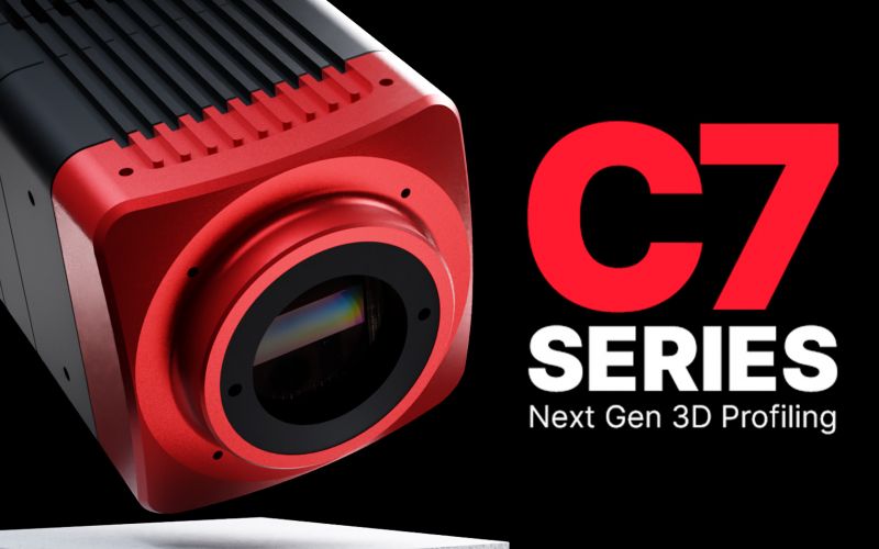
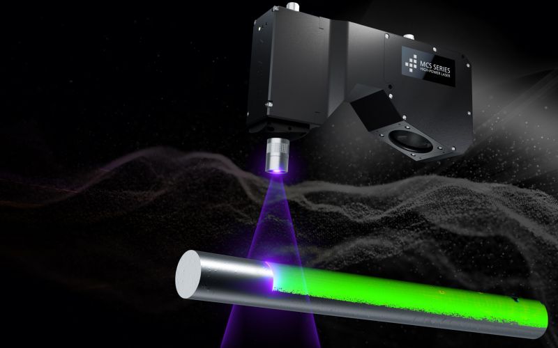
The WARP sensor is actually available in all our cameras and sensor models. In addition, thanks to the modular design of our MCS family, we can produce a customized sensor for every customer without any development costs. So there are no limits to the use of the WARP sensor other than physics.
9. What is the cost-benefit ratio of the new sensors compared to conventional sensors?
The good news is that our customers get up to 10 times higher readout rates without having to pay anywhere near 10 times higher costs . That is already very positive for the cost-benefit ratio. So far, we have received very positive feedback on the prices of this series. However, AT sensors cover a wide range of applications. For example, we already offer high-performance 3D sensors from EUR 5,500 with our “ECS” economy series.
10. What plans does AT Sensors have for the further development of 3D technology?
We actually still have a lot of ideas and plans that go beyond the chip to include laser technology, the overall design of the sensors and, of course, the software. Last year, we launched three new product series and will continue to introduce further innovations for our customers in 2025!
Thank you very much for your time and for answering our questions.


